Invisible Connections will Unveil our 5G Future

At Signal Microwave, simulation is being used to design specialized connectors for high-speed RF applications.
The following is an excerpt from Multiphysics Simulation 2017 . By: Sarah Fields As the number of mobile users and the demand for high speed communication grows, companies and industry groups are working around the clock to rise to the challenge.
The 5G network aims to be 100 times faster than 4G LTE and increase broadband connection speeds by 10 times. “There are a lot of moving pieces that need to arrive at the same place in order for 5G to move from concept to reality,” says Bill Rosas, cofounder of Signal Microwave. “Those on the front line not only have to implement the 5G, they need to figure out everything from testing the networks to updating the interconnects in their systems.”
The small details of connectors are worthy of significant R&D focus. These indispensable electromechanical parts used to join electrical terminations, which can transfer electromagnetic energy from one transmission line to another component for transmission or interpretation.
Connectors are omnipresent across all electronic devices and systems, and their precision is critical in circuits that transmit information, especially as data transfer rates increase.
Eric Gebhard and Bill Rosas cofounded Signal Microwave in order to provide specialized connectors for the signal integrity market on demand.
By anticipating the need for optimized RF, microwave, and millimeter-wave connectors for circuits transmitting higher and higher data transfer rates, Signal Microwave will support the development of our 5G future.
THE COMPLEXITY OF INCREASED FREQUENCY
Those working on RF (radio frequency) connectors face a multifaceted set of design hurdles, as geometry, size, and transmission constraints must be met while matching the impedance of the connector to the rest of the transmission line. “The component manufacturers have been very quick in offering products for 5G applications,” says Rosas.
“But providing components that are highly optimized is where the opportunities lie.” As the frequency increases, maintaining the impedance becomes more complex, as small quirks arising from the geometry or selected materials can be magnified.
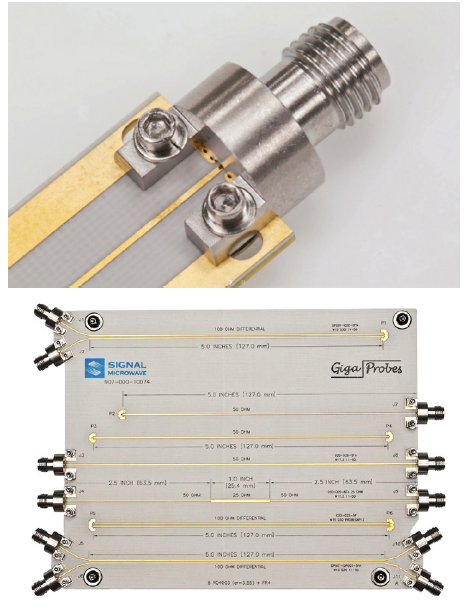
Figure 1 shows a photo of an RF connector designed for a 5G communications application under development.
Gebhard and Rosas were interested in ways that these critical pieces of RF infrastructure could be further optimized through the use of simulation.
Signal Microwave’s customers are far ranging and include engineers developing high-frequency applications for the communication sector, commercial market, and military, from 40 GHz to 110 GHz.
DESIGNING AN RF CONNECTOR
Multiphysics simulation has enabled Eric and his team to swiftly meet the design challenges that accompany each new customer. “The software can interface with other design tools, which has allowed our team to rapidly develop optimized connectors that meet the individualized requirements of the diverse industries our customers represent,” said Gebhard.
This approach reduces time to market, overall development costs, and required investment, allowing device designers to focus on other critical aspects of the design knowing they can safely rely on the connecting components. Simply stated, the designer of an electrical connector takes a mechanical part and turns it into a transmission line.
The goal in designing an RF connector is to build a part that is electrically invisible, making it indistinguishable from the rest of the transmission line which means meeting minimum requirements for resistance and energy loss.
“We’re interested in minimizing mismatches causing reflections, which results in distortion or a diminished signal,” says Gebhard. Simulation offers a way to do this before fabrication and testing.
CHASING THE PERFECT CONNECTION WITH SIMULATION
Signal microwave’s customers often require specific geometric parameters for one part of the connector as well as a predetermined impedance, which then informs the rest of the design.
Gebhard and Rosas take a holistic approach to connector design and consider the requirements for the circuit board and device in their entirety before beginning the design of the connector.
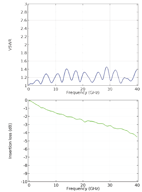
The team typically starts by building the geometry in Solid Edge® software and importing it into COMSOL Multiphysics® software, where they can use the RF modeling functionality to analyze and optimize the design. Simulation allows Gebhard to investigate the measured voltage standing wave ratio (VSWR), reflection and insertion loss, or power loss due to mismatches or unexpected discontinuity, which must be minimized.
For example, the measured voltage standing wave ratio (VSWR) of a test circuit board with Signal Microwave components matched simulation results and was found to be less than 1.5:1, indicating sufficiently low reflectance and loss (Figure 2, top). It was determined that the losses are not drastic and increase gradually as the frequency goes up (Figure 2, bottom).
With multiphysics simulation, the team at Signal Microwave has created a portfolio of solderless edge connectors that feature minimal reflections, which can be extended to the millimeter-wave range.
EDGE-LAUNCH CONNECTORS GET EXCITED
GEBHARD ALSO MODELED two edge-launch connectors, excited and terminated by 50-ohm coaxial lumped ports. In this example, the grounded coplanar waveguide (GCPW) circuit board was built with an 8-mils substrate with a dielectric constant of 3.55.
Metalized vias connect the pair of ground planes of the CPW to the bottom ground plane (Figure 3).
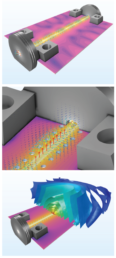
“In order to make a connector electrically invisible we minimize reflection, described by scattering parameters, by looking at geometric discontinuities,” says Gebhard. In addition to adjusting the geometry to minimize reflection, Gebhard may also optimize the dielectric materials to obtain the desired impedance.
In certain cases, Gebhard will use the COMSOL® software to evaluate additional structural design considerations, such as the minimum force required to remove the pin from the main frame of the connector.
A CLOSE MATCH TO REALITY
Gebhard also developed 70-GHz blind mate connectors used for automated test equipment. After creating the RF model in the software, he had the prototypes built. Surprisingly, the prototype connectors did not work as expected.
Gebhard took a closer look at the machined prototype and realized there was a small defect in one connector. In a bit of forensic engineering, Gebhard then returned to the original model and added the defects into the model. Lo and behold, the simulation then matched the physical test results.
“The virtual design was right, but the parts weren’t and we didn’t catch that. Once we tested it and looked at the parts closely, we found the problem.
We then put the defect into the virtual model, and saw the simulation results match what we were seeing. You could say it was one of our ‘Eureka’ moments. “In this case especially, I was very happy to see the simulation results so closely match reality. In this RF connector design, we had added a few unique aspects, which made us eager to see how the connector would perform.”
High-fidelity simulation allowed Gebhard the freedom to design and build custom connectors for specialized RF applications, reducing the number of physical prototypes and speeding up development time.